Bonding Copper Wire
Silicon Carbide (SiC) Foam Ceramic Filter is a porous ceramic product featuring a three-dimensional interconnected network structure. It uses silicon carbide as the primary matrix material and is manufactured by replicating the structure of organic foam through a specialized process followed by high-temperature sintering. This filter combines the excellent properties of SiC ceramic with the high specific surface area of porous materials, making it a critical functional component in fields such as molten metal filtration and high-temperature gas purification.
Request a Quote
Take the next step to forging your path to success. Request a quote from our team.
Quality Assurance
Ensuring that our processes and products meet international quality and safety requirements.
Feature
| Feature | Description | Key Advantage |
| Material Purity | 4N (99.99%) or higher high-purity copper | Ensures consistent electrical stability and low impurity levels. |
| Diameter Range | 15μm – 50μm (0.6 mil – 2.0 mil) | Supports both ultra-fine pitch and high-power packaging. |
| Electrical Conductivity | ~103% IACS (International Annealed Copper Standard) | Higher than gold; reduces heat generation in high-current devices. |
| Thermal Conductivity | ~390 – 400 W/m·K | Superior heat dissipation, extending the lifespan of the chip. |
| Tensile Strength | 200 – 300 MPa (depending on annealing) | High stiffness prevents “wire sweep” during the molding process. |
| Elongation | 8% – 15% | Balanced flexibility for stable looping and high-speed bonding. |
| IMC Stability | Slower Intermetallic Compound growth (Cu-Al) | Enhanced long-term reliability in high-temperature environments. |
| Surface Finish | Ultra-smooth with anti-tarnish treatment | Prevents oxidation and ensures consistent capillary feeding. |
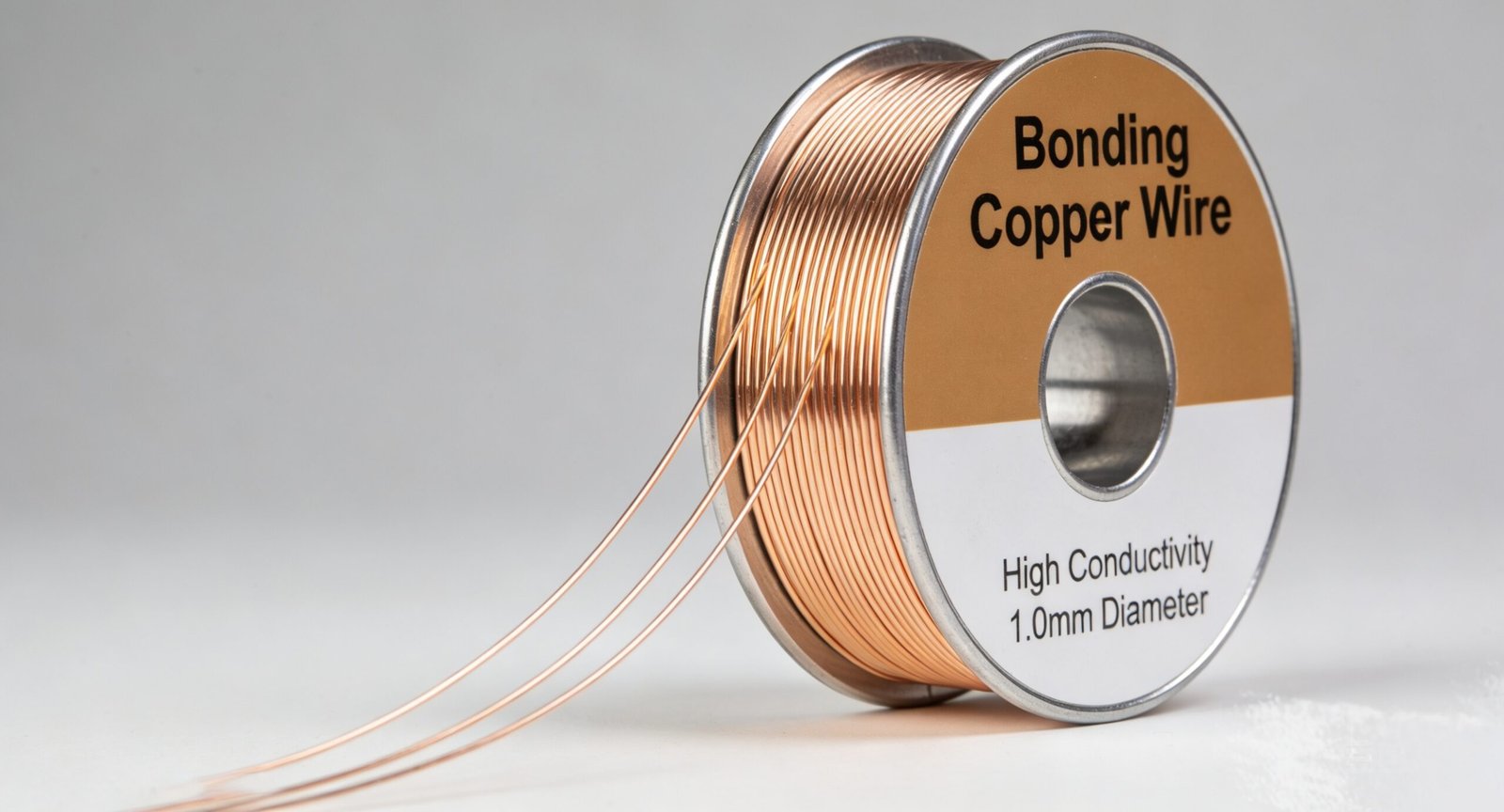
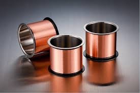
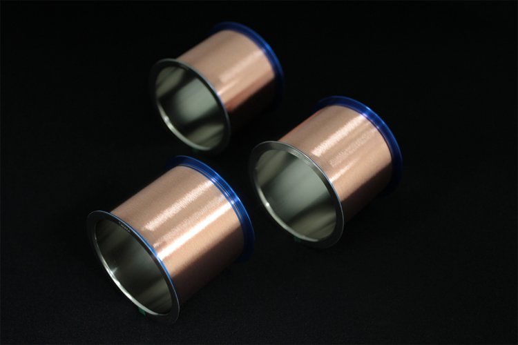
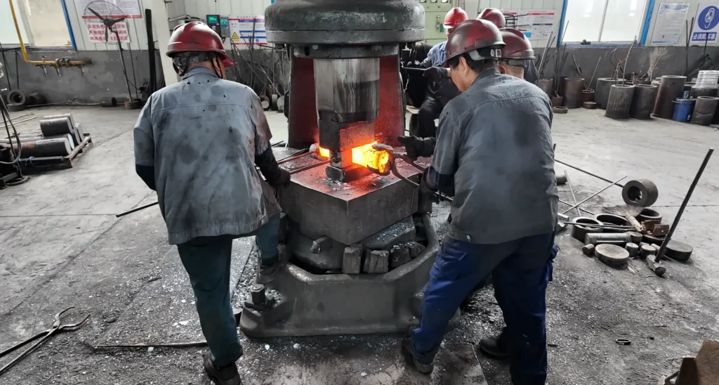
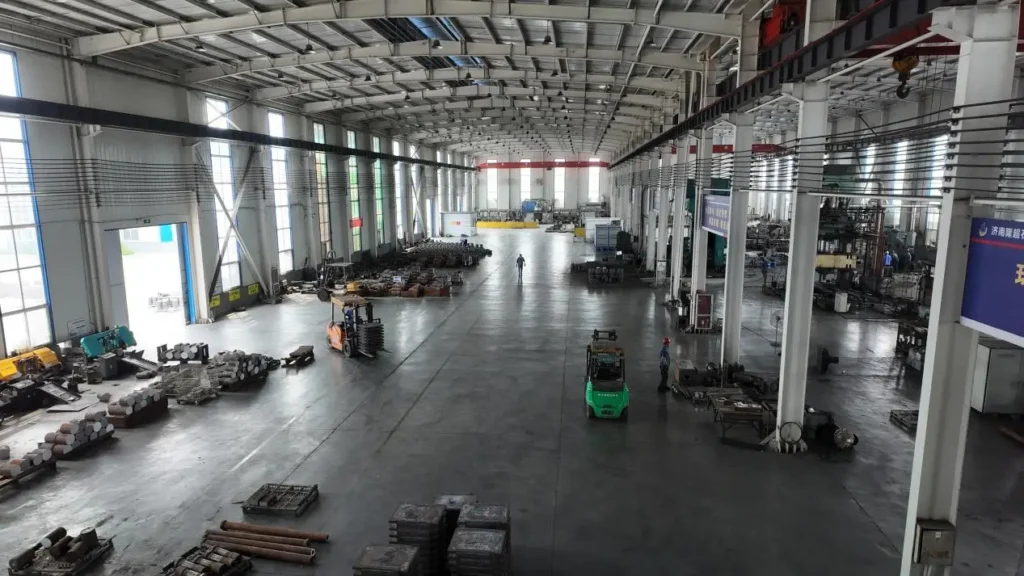
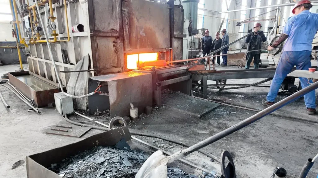
Explore Our Bonding Copper Wire
| Wire Category | Diameter Range (μm) | Typical Applications | Key Selection Criteria | Bonding Method |
| Ultra-Fine Pitch | 15μm – 20μm | High-density Memory, Smart Cards, Mobile CPUs | Highest wire sweep resistance; Low loop profile. | Thermo-sonic Ball Bonding (N2/H2 gas) |
| Standard IC | 23μm – 33μm | Consumer Electronics, MCUs, Logic ICs | Balanced conductivity and cost; High-speed bonding stability. | Thermo-sonic Ball Bonding (N2/H2 gas) |
| Power & Discrete | 38μm – 50μm | Power Transistors, MOSFETs, Schottky Diodes | Maximum thermal dissipation; High current carrying capacity. | Heavy Wire Wedge/Ball Bonding |
| High Reliability | 25μm – 30μm | Automotive Electronics, Industrial Controls | Superior IMC stability; Enhanced long-term heat resistance. | Optimized Capillary & Gas Shielding |
| LED Packaging | 20μm – 25μm | Mid-to-High Power LEDs, Display Modules | High reflectivity; Excellent heat dissipation for longevity. | Standard Ball Bonding |
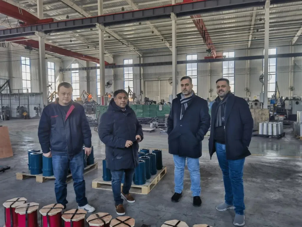
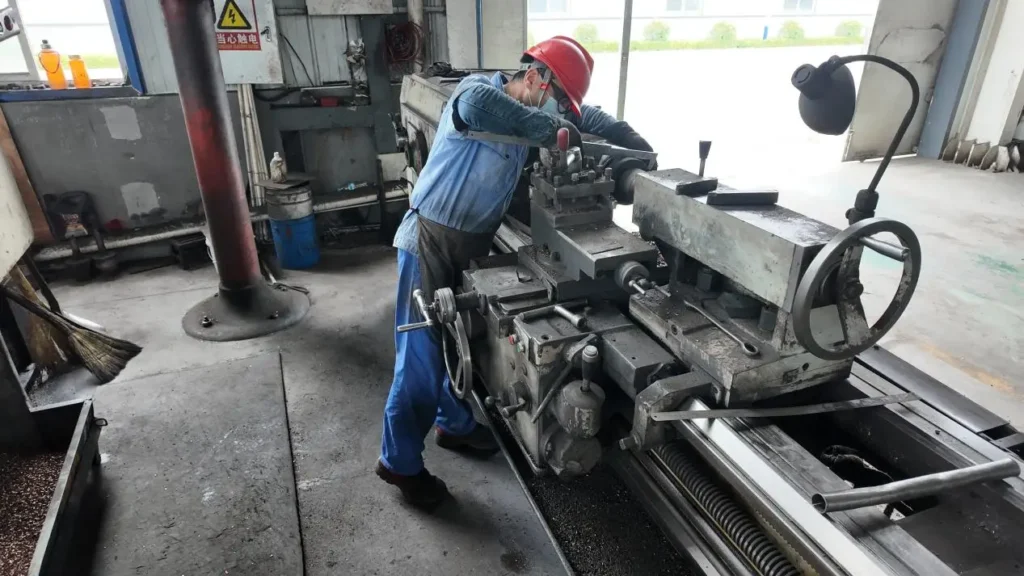
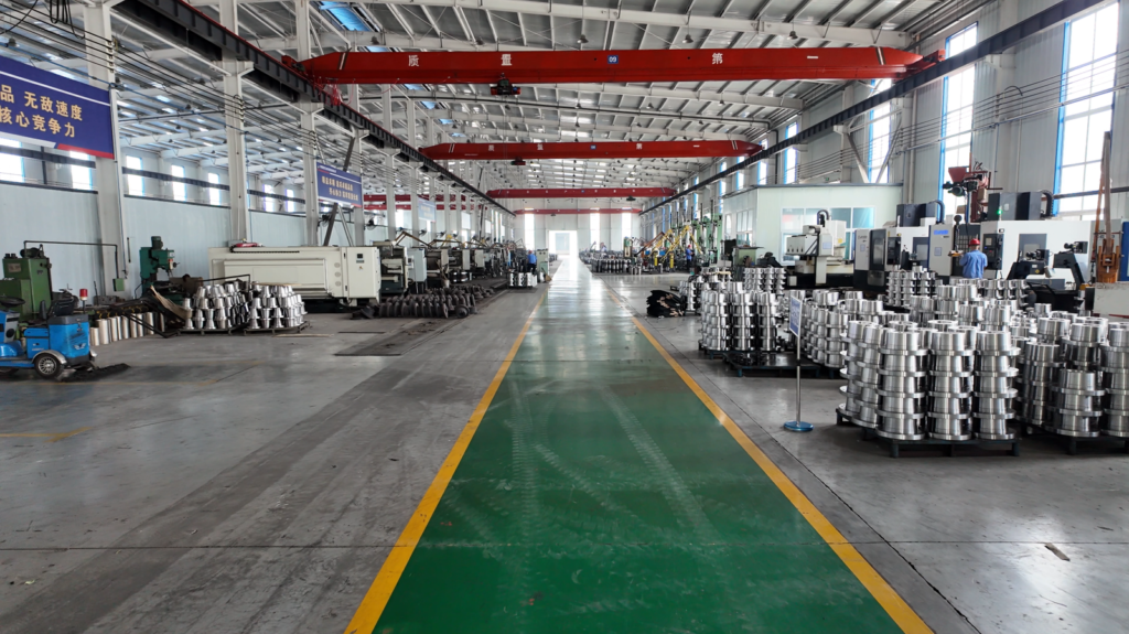
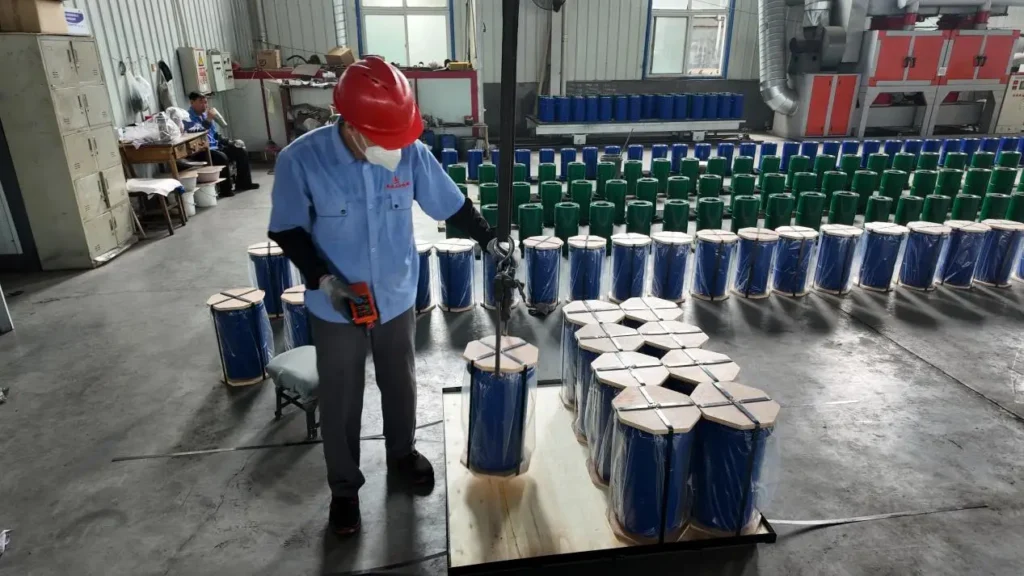
BI-METAL LINER & Seat & Spare Parts – Buyer FAQs
What are the primary benefits of switching from Gold to Copper wire?
The most significant benefit is 70-90% cost reduction in material. Additionally, copper offers ~25% higher electrical conductivity and superior thermal dissipation, which improves device performance.
Does Copper wire require different equipment than Gold wire?
Most modern automatic ball bonders are “copper-ready.” However, you must install a gas delivery system to provide a shielding gas (typically 95% N2 / 5% H2) to prevent oxidation during the Free Air Ball (FAB) formation.
How does the hardness of Copper affect the silicon chip?
Copper is harder than gold. To prevent Pad Cratering (chip damage), it is essential to use optimized bonding parameters (lower impact force) and ensure the Aluminum pad thickness is sufficient (ideally >1.0μm).
What is the typical shelf life of Bonding Copper Wire?
Due to copper’s susceptibility to oxidation, the shelf life is typically 6 months in original vacuum-sealed packaging. Once opened, it should be used within 24 hours or stored in a nitrogen cabinet.
Can Copper wire be used for automotive or high-reliability apps?
Yes, but for extreme reliability, Palladium-Plated Copper (PCC) is often preferred. It offers superior resistance to corrosion and intermetallic (IMC) degradation compared to bare copper
Advantages
The superior performance of Bare Copper Wire stems from its high-purity metallic properties and precisely controlled crystalline architecture. This combination ensures exceptional electrical conductivity and thermal dissipation to minimize internal resistance, while its high-modulus characteristic provides the structural rigidity needed to resist wire-sweep during molding. By forming high-strength intermetallic compounds (IMC) through optimized grain structures, Bare Copper delivers superior interface bond strength and significant cost-efficiency for high-speed semiconductor packaging.
High-Precision Drawing & In-line Annealing Process
This manufacturing process utilizes a high-precision multi-stage drawing method, uniformly reducing the diameter of 4N/5N high-purity copper rods through diamond dies. After precise structural elongation and controlled in-line annealing, the wire is stabilized in a vacuum furnace at optimized temperatures, causing the copper grains to recrystallize into a uniform equiaxed structure, forming a robust, high-conductivity electrical connection path.
These cost-saving advantages, combined with superior electrical conductivity, can mean better production rates and higher efficiency for your semiconductor operations. When you succeed, we know we've succeeded.
Research
"Our R&D focuses on micro-alloying and multi-layer composite coating designs to overcome copper’s inherent hardness and oxidation, achieving bonding reliability that rivals gold wire."
Experiment
"Through rigorous uHAST (Highly Accelerated Stress Test) and microscopic interface analysis, we quantify bond-point consistency and long-term stability under extreme high-temperature and high-humidity environments."
Production
"Utilizing continuous drawing and precision in-line annealing within a Class 10,000 cleanroom, we ensure micron-level diameter tolerances and coating uniformity for high-volume, high-quality production."
Application
"As a cornerstone for cost-efficiency in power electronics and automotive modules, our solutions leverage superior thermal and electrical conductivity to meet the demands of high-density, high-power advanced packaging."
Jinan Zunbo CNC Technology Co., Ltd.
The company has successfully obtained various domestic and international quality system certifications—including ISO9001, ISO14001, and IATF16949—and has passed all relevant product testing standards.
